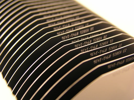
The global wafer fabrication market is expected to grow from USD 50.56 billion in 2018 to USD ~62 billion by 2025, at a CAGR of ~4% during the forecast period. The process of producing electronic integrated circuits (IC) is complex. The equipment used for wafer fabrication includes epitaxial deposition equipment, oxidation systems, diffusion systems, ion implantation equipment among others.
FREE Sample@ https://www.marketresearchfuture.com/sample_request/8401
Silicon is the most common semiconductor used for wafer fabrication process. Increasing demand for electronic and electrical devices and the growth of the automotive industry are the major factors contributing to the growth of the global wafer fabrication market.
Regional Analysis
The global wafer fabrication market is projected to grow at a significant rate during the forecast period from 2019 to 2025. The geographic analysis of the global wafer fabrication market has been conducted for North America, Europe, Asia-Pacific, the Middle East and Africa, and Central and South America.
Asia-Pacific dominated the wafer fabrication market in 2018 due to the presence of major players in countries such as Japan and China. Also, the governments of the countries in the Asia-Pacific region are supporting the players operating in the market. North America is expected to be the fastest-growing region during the forecast period due to high adoption of IoT, artificial intelligence, and connected devices across industry verticals in the region. The market in Europe is expected to show significant growth owing to presence of a widespread automotive market in the region. The markets in the Middle East and Africa and Central and South America are expected to show significant growth in wafer fabrication market in coming years.
Segmentation
The global wafer fabrication market has been segmented on the basis of equipment type, fabrication process, end user, and region.
Based on equipment type, the global wafer fabrication market has been segmented into oxidation systems, diffusion systems, epitaxial reactors, photolithography equipment, ion implantation equipment, and others.
By fabrication process, the global wafer fabrication market has been classified as front end of line processing and back end of line processing.
Key players
The key players in the global wafer fabrication market are Lam Research Corporation (US), SCREEN Semiconductor Solutions Co., Ltd (Japan), Tokyo Electron Limited (Japan), SAMSUNG (South Korea), Applied Materials, Inc. (US), Hitachi High-Technologies Corporation (Japan), Motorola Solutions, Inc (US), Intel Corporation (US), KLA-Tencor Corporation (US), and ASML Holding NV (Netherlands).
Other prominent players studied for the global wafer fabrication market are Dainippon Screen Manufacturing Co. Ltd. (Japan), Nikon Corporation (Japan), Taiwan Semiconductor Manufacturing Company Limited (Taiwan), Merck KGaA (Germany), and Okmetic Oy (Finland) among others.
“Don’t miss out on business opportunities in Wafer Fabrication Market. Get detailed report and gain crucial industry insights that will help your business grow.”
https://www.marketresearchfuture.com/reports/wafer-fabrication-market-8401
Other Related Market Research Reports:
ECC Memory Market Research Report – Global Forecast till 2025
https://www.marketresearchfuture.com/reports/ecc-memory-market-8335
| https://www.marketresearchfuture.com/reports/wafer-fabrication-market-8401 |
Media Contact
Company Name: Market Research Future
Contact Person: Abhishek Sawant
Email: Send Email
Phone: +1 646 845 9312
Address:Market Research Future Office No. 528, Amanora Chambers Magarpatta Road, Hadapsar
City: Pune
State: Maharashtra
Country: India
Website: https://www.marketresearchfuture.com/reports/wafer-fabrication-market-8401

