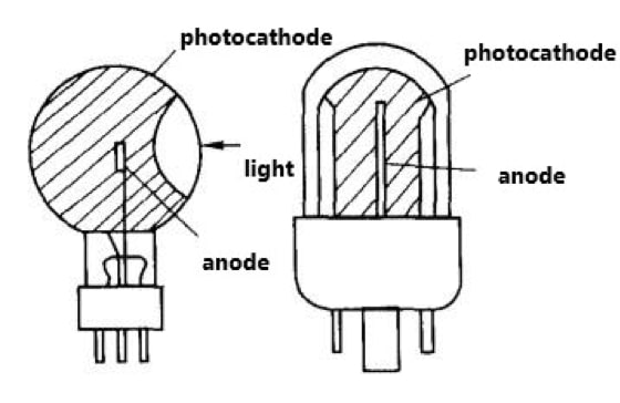
The photoelectric sensor is a kind of converter that converts the change of light quantity into the change of electric quantity. It has a wide range of applications and has been used in various fields such as aerospace, medicine, scientific research, industrial control, household appliances, and navigation. The theoretical basis of the photoelectric sensor is the photoelectric effect, and various photoelectric sensors can be made according to the photoelectric effect. Today, Easybom will introduce the basic theoretical knowledge of the photoelectric effect in detail. In the early days, people used the photoelectric effect to make photocells. Its shape and structure are shown in the figure below. It is an evacuated glass bubble with a part of the inner wall of the bubble coated with metal or metal oxide, which acts as the cathode of the photocell. The anode of a photocell is a thin ring-shaped metal wire or a semicircular metal ball.

Photocell Structure
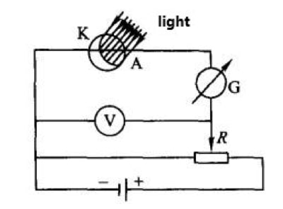
The experimental setup of the photoelectric effect is shown in the figure below. The anode A of the photocell is connected to a high potential, and the cathode K is connected to a low potential, there is an accelerating electric field between the anode and the cathode, and the direction of the electric field is from A to K. The voltage between AK is read out by the voltmeter V, and the magnitude of the voltage is given by the potentiometer R. In the figure, G is a sensitive galvanometer. Experiments show that when the cathode is not illuminated by light, there is almost no current in the circuit; when the cathode is illuminated by light, there is an immediate current in the circuit. As long as the light is illuminated, the current will be maintained for as long; when the light stops, the current will disappear. This means that electrons escape from the photocathode when light is illuminated. Under the action of the accelerating electric field, the electrons fly to the anode, thereby forming a photocurrent in the circuit.

Experimental Setup for the Photoelectric Effect
Substances released electrons under the action of light, which is a phenomenon called the photoelectric effect. The photoelectric effect is usually divided into two categories: the external photoelectric effect and the internal photoelectric effect.

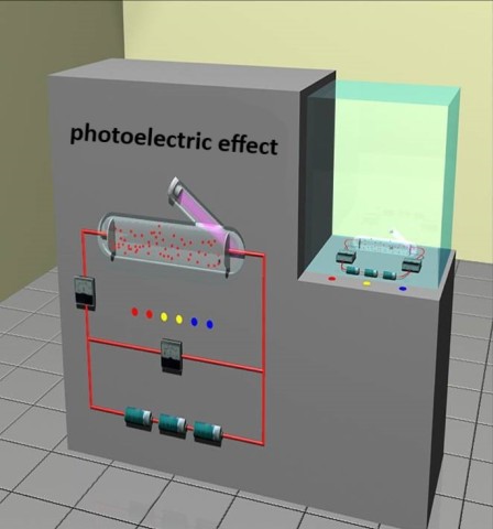
Photoelectric Effect
1. External Photoelectric Effect
Under the action of light, the electrons in the object escape from the surface of the object and emit outward, which is called the external photoelectric effect. Photoelectric devices based on the external photoelectric effect include photocells, photomultiplier tubes, etc.
2. Internal Photoelectric Effect
The electrical conductivity of the illuminated object changes or generates a photoelectromotive force, which is called the internal photoelectric effect. The internal photoelectric effect can be divided into the following two categories.
1) Photoconductive effect
Under the action of light, electrons absorb photon energy and transition from a bonded state to a free state, causing a change in the resistivity of the material. This phenomenon is called the photoconductive effect. The vast majority of high-resistivity semiconductors have photoconductive effects. Photoelectric devices based on this effect include photoresistors (also called photoconductors), and their commonly used materials are cadmium sulfide (CdS), lead sulfide (PbS), indium antimonide (InSb), amorphous silicon (a-Si: H).
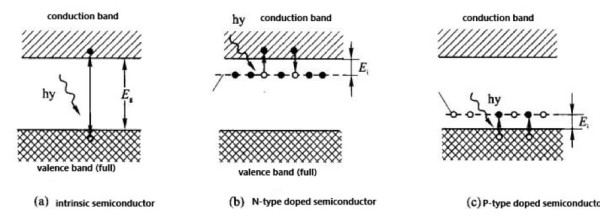
Under the irradiation of light, electrons in the forbidden band of pure semiconductors are excited by photons with energy greater than or equal to the forbidden bandwidth Eg (eV), and transition from the valence band to the conduction band, becoming free electrons. At the same time, the valence band also forms free holes. As a result, the concentration of electrons in the conduction band and holes in the valence band in pure semiconductors increases, and the resistivity of the semiconductor decreases. As shown in Figure (a) below. Electrons and holes are collectively called carriers. They can form photocurrent under the action of terminal voltage. When the light is stopped, free electrons are captured by atoms that have lost electrons, and the resistance returns to its original value. In the spectral range where electrons in the valence band can transition to the conduction band, the maximum wavelength λ0 (nm) is called the cutoff wavelength, and λ0≈1240/Eg.
N-type or P-type doped semiconductors are illuminated by light, as long as the photon energy is greater than the difference between the donor energy level and the bottom conduction band energy level or the difference between the acceptor energy level and the top energy level of the full band Ei(eV), as shown in Figure (b) or Figure (c), light energy is absorbed, and photogenerated electrons or holes that can participate in conduction are excited. The cut-off wavelength of photogenerated carriers generated by the doped semiconductor is λ0≈1240/Ei.

Photoconductive Effect Mechanism Diagram
When the photoresistor is connected to the DC voltage Vb and continuously irradiated with light with a certain intensity and wavelength less than λ0, the output DC current i0 is

In the formula, η-the internal photon quantum efficiency (the ratio of the number of photogenerated carriers to the number of emitted photons); μc-the mobility of the majority carriers; τ – the lifetime of the majority carriers; d-the distance between the two electrodes of the photoresistor; p-incident optical power; e – Planck’s constant, which is 6.6261×10⁻³⁴J•s.
With the increase of light energy, although the concentration of photogenerated carriers also increases sharply, the recombination speed between electrons and holes is also accelerated, so the characteristic curve of light energy below the cut-off wavelength and the photocurrent generated by the semiconductor is not the linear relationship.
2) Photovoltaic effect
The phenomenon that an object (such as a semiconductor) can generate an electromotive force in a certain direction under the irradiation of light is called the photovoltaic effect. Photoelectric devices based on this effect include photocells, photodiodes, and phototransistors.
The photovoltaic effect can be divided into:
• Lateral photovoltaic effect
The lateral photovoltaic effect is also known as the Dember effect.
When the photosensitive surface of the semiconductor optoelectronic device is illuminated unevenly, the photoelectric effect caused by the carrier concentration gradient is called the lateral photovoltaic effect. Optoelectronic devices that work based on this effect include semiconductor position-sensitive devices (PSD for short), or inversion photodiodes.
The working mechanism of the lateral photovoltaic effect is that the illuminating part of the semiconductor absorbs the energy of the irradiated photons to generate electron-hole pairs, so that the carrier concentration in this part is higher than that in the unilluminated part, so a concentration gradient occurs, forming a carrier diffusion. Since the mobility of electrons is larger than that of holes, electrons first diffuse to the unilluminated part, so that the illuminated part is positively charged, the unilluminated part is negatively charged, and a photoelectromotive force is generated between the two parts.
• PN junction photovoltaic effect
When light strikes a semiconductor PN junction very close to the surface, the junction and nearby semiconductors absorb the light energy. If the photon energy is greater than the forbidden bandwidth, the electrons in the valence band transition to the conduction band and become free electrons, and the valence band correspondingly becomes free holes. Under the action of the electric field inside the PN junction, the electrons move to the outside of the N region, and the holes move to the outside of the P region. As a result, the P region is positively charged, and the N region is negatively charged, forming a photoelectromotive force.
The photogenerated current of the PN junction is proportional to the illuminance, and the photovoltaic voltage is proportional to the logarithm of the illuminance.
Since photogenerated electrons and holes will recombine with semiconductor holes and electrons respectively during the diffusion process, the lifetime of carriers is related to the diffusion length. Only if the thickness of the PN junction from the surface is smaller than the diffusion length, the photocurrent can be formed to generate photovoltaics. In engineering, by changing the thickness of the PN junction from the surface, the frequency response characteristics, photocurrent, and photoelectric potential of optoelectronic devices based on the PN junction photovoltaic effect can be adjusted.
Photoelectric devices based on this effect include photovoltaic cells, solar cells, photodiodes, and phototransistors. Through the design and manufacturing process, the photovoltaic cell works with a photovoltaic effect without an external power supply. When the photosensitive tube works under reverse bias, both photoconductive effect and photovoltaic effect exist. The photocurrent they output has a linear relationship with the light intensity.
• Photoelectromagnetic effect (referred to as PEM effect)
When a semiconductor is irradiated by strong light and a magnetic field is applied in the vertical direction of the illumination, the phenomenon that an electric potential is generated between the two ends of the semiconductor perpendicular to the light and the magnetic field is called the photoelectromagnetic effect. It can be regarded as the Hall effect of light diffusion current.
• Becquerel effect
The Becquerel effect is a photovoltaic effect in liquids. When light irradiates either of two identical electrodes immersed in an electrolyte, the phenomenon that an electric potential is created between the two electrodes is called the Becquerel effect. There are photosensitive cells based on this effect.
Website: https://www.easybom.com | Email: info@easybom.com
Media Contact
Company Name: Easybom, Inc.
Contact Person: Jack Smith
Email: Send Email
Phone: +1 (718) 737-2822
Address:506 2nd Ave. Ste 1600
City: Seattle
State: WA 98104
Country: United States
Website: https://www.easybom.com

