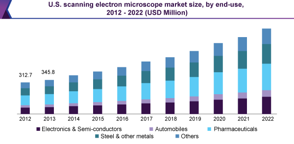
According to a report published by Grand View Research, Inc.; the scanning electron microscopes (SEM) market is expected to reach a valuation of around USD 2.9 billion by 2022.
Increasing demand of nanotechnology-based research and growing application in semiconductor, electronics and pharmaceutical industries can drive the market during the forecast period (2012 to 2022). In addition, advancements in the resolution power and attachment of other devices like energy x-ray dispersion spectrometer can also boost the market.
Technological developments in SEM has improved the quality control procedures of research laboratories in various industries including semiconductors, pharmaceutical, automobiles. These microscopes play an important role in imaging and elemental analysis of products. The advanced SEMs offer several advantages like high resolution, compact size, rapid analysis, and 3D imaging. In addition, they provide data about surface morphology and properties like topography, fractography, and chemical analysis. This has increased the demand across pharmaceutical companies and small to medium scale R&D. Increasing focus on R&D for applications including material sciences, life sciences, neurosciences, nanotechnology, and semiconductor industry are likely to increase use of automated microscopes such as analytical electron microscope, scanning electron microscopes, scanning probe microscope. These microscopes deliver high imaging resolution around 0.1 nm, which is required in precision manufacturing industries.
Full Research Report On Scanning Electron Microscopes Market Analysis: www.grandviewresearch.com/industry-analysis/scanning-electron-microscope-market

Worldwide scanning electron market microscopes market can be segmented on the basis of end-use and region. As per end-use, the market can be categorized into electronics and semiconductors, automobiles, pharmaceuticals, steel and other metals, and others. The pharmaceuticals segment is expected to grow over 30.0% share by 2022 due to high prevalence of chronic diseases, which has increased R&D investments and high demand for digital microscopes in areas like medicine and life sciences. The automobiles segment is likely to grow at a lucrative CAGR of over 11.0% during the forecast period. Increasing use of SEM in surface observation, coating analysis, film thickness analysis, fractography, and failure analysis of metallic and non-metallic parts can drive the segment growth. The semiconductor segment is also expected to grow at significant rate in the coming years. SEMs are used un semiconductor device manufacturing for procedures including failure analysis and detection, and semiconductor device manufacturing. Growing trend of miniaturization of transistor chips, which requires advanced microscopes including TEM, SPM, and SEM, for analytical and quality assurance is also expected to drive the market in the coming years.
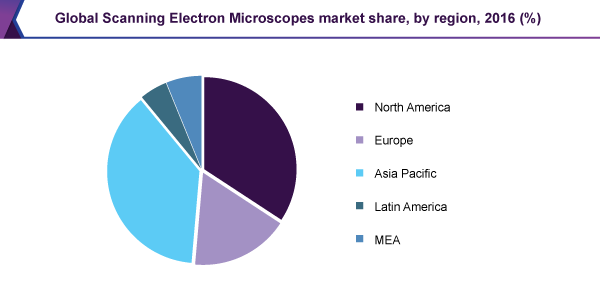
Geographically, the market can be divided into North America, Europe, Asia Pacific, Latin America, and Middle East and Africa.
Browse More Reports Of This Category By Grand View Research At: www.grandviewresearch.com/industry/medical-devices

In 2014, Asia Pacific estimated for the major market share of over 38.0%. Robust growth in application such as automobiles, semiconductor, nanotechnology, and pharmaceuticals are driving the growth in this region. This region is likely to dominate the market through 2022 due to presence of established manufacturing and growing use of SEM for imaging and elemental analysis. In addition, rapid growth of semiconductor industry in emerging countries such as China and India due to rise in outsourcing of electric equipment manufacturing is considered as the key driving factor in this region.
In 2014, North America was the second largest market and estimated for 36.10% share due to existence of research and academic institutes and increasing number of clinical trials in the region. Increasing research activities in life sciences, biotechnology and pharmaceutical industries are likely to increase product demand in this region over the forecast period. Increasing funding for nanotechnology-based application is also expected to drive the market growth in this region. As per the U.S. National Nanotechnology Initiative, public investment in nanotechnology grew zero in 2000 to about USD 65 billion in 2011.
Latin America is expected to grow on account of increasing demand for advanced SEM in several material research in this region. This region is expected to expand with a CAGR of 11.6% during the forecast period.
Key players operating in the market include Nanoscience Instruments, Inc.; Olympus Corporation.; Hitachi High Technologies Corporation.; Bruker Corporation; and Hitachi High Technologies Corporation.
Major market participants are making high investment in R&D of SME and following strategies such as new product launch, mergers and acquisitions to sustain in the market.
Explore the BI enabled intuitive market research database, Navigate with Grand View Compass, by Grand View Research, Inc.
About Grand View Research
Grand View Research, Inc. is a U.S. based market research and consulting company, registered in the State of California and headquartered in San Francisco. The company provides syndicated research reports, customized research reports, and consulting services. To help clients make informed business decisions, we offer market intelligence studies ensuring relevant and fact-based research across a range of industries, from technology to chemicals, materials and healthcare.
For more information: www.grandviewresearch.com
Media Contact
Company Name: Grand View Research, Inc.
Contact Person: Sherry James, Corporate Sales Specialist – U.S.A.
Email: Send Email
Phone: 1-415-349-0058, Toll Free: 1-888-202-9519
Address:28 2nd Street, Suite 3036
City: San Francisco
State: California
Country: United States
Website: www.grandviewresearch.com/industry-analysis/scanning-electron-microscope-market

