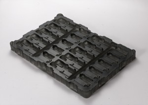
Main purpose: Eliminate static electricity, which is widely used in the turnover loading, packaging, storage and transportation of electronic devices and product production processes. In the industry, it is also called static conductive tray; the height of the tray is generally below 100mm; it is suitable for the storage container of precision electronic components. According to the requirements of customers’ electronic components, there are also different requirements for the size.
An anti-static tray is an ideal tool for storing electronic components. The finished product has good mechanical strength and heat resistance; good impact resistance and strong chemical resistance. Will not change its anti-static performance due to environment, time and temperature.

The anti-static tray can effectively release the static charge accumulated on the surface of the object, so that it will not generate charge accumulation and high potential difference; it can greatly reduce the damage rate of electronic products in the production process, reduce costs, and improve product quality and profit.
Classification
1. Anti-static tray
2. Conductive tray
3. Anti-static tray for parts
Structure classification
1. Stackable anti-static tray
2. Sub-format anti-static tray
3. Anti-static tray with holes
4. Hollow board anti-static tray
Performance
It has flexural resistance, aging resistance, high load-bearing strength, tensile, compression, tearing, and high temperature. It can be made into a box-type turnover box that can be used for both turnover and finished product shipment packaging. It is lightweight, durable, and stackable. Various specifications and sizes can be customized according to user needs and can be equipped with a cover, dust-proof, anti-static, and beautiful in appearance. Generally, anti-static trays are designed and manufactured according to the size provided by the customer to achieve the most reasonable loading, and multiple trays can be overlapped, effectively using the plant space, increasing the storage volume of electronic components, PCB boards, and dust-free workshop parts, and saving production costs.
Media Contact
Company Name: Shenzhen Kingsmart Industrial Development CO., LTD
Email: Send Email
Phone: 00868615112665631
Country: China
Website: https://www.kingblister.com/
